-
 Load Cell Sensor Introduction
- Date Tue 02 August 2016
- By Jason Jones
- Category load-cell-sensor
- Tags load-cell-sensor project load-cell sensor wheatstone bridge msp430

Load Cell Amplifier
I was browsing Sparkfun a few days ago and came across their OpenScale board. The board is basically a load-cell amplifier with a microcontroller interface which will output data - via an FTDI chip - to the PC or other UART at a fixed interval. The microcontroller also has the ability to read local and - if present - remote temperature sensors. I was about to purchase the item when I realized that it was $29.95... what!!!
That is when I remembered coming across a TI microcontroller, the MSP430AFE251 which has an integrated 24-bit sigma-delta ADC with a programmable gain amplifier. In addition, it has an on-board temperature sensor. Basically, it has everything that the Sparkfun board has EXCEPT for a USB interface. It looks like a new project time! It looks like I could make one of these for ~$10 in single-piece quantities and quite a bit less for higher quantities.
Load Cell Tutorial
In electronics-speak, you want to have an amplifier that can read the voltage difference from a Wheatstone bridge with enough resolutions to obtain meaningful data.
Sparkfun's Getting Started with Load Cells tutorial does a pretty good job of going through the basics of load cells and how to use them, so - if you have questions - go there. We are going to focus on the electronics required to get the job done.
Electronics
Basic Requirements
Sigma-Delta Converter
The most basic building block is the analog-to-digital converter (ADC). The sigma-delta ADC is the standard in high-precision converters because you can get so many bits of resolution from them. If you don't need the resolution, you can use the faster and more standard successive approximation ADCs which are standard on most microcontrollers.
Programmable Gain Amplifier (PGA)
If you have a 64-bit converter, then you probably don't need the PGA. If you don't, then you will likely need some analog interface which will allow you to increase the gain of the differential input before the ADC. The amplifier can take the form of a fixed amplifier, but - with the microcontroller interface - it would be nice to have the amplifier be programmable so that we can reduce the gain under saturation conditions and increase the gain when the signal is too small.
Microcontroller
Of course, we are converting analog data to a digital format, so we need to have some method of translating. The microcontroller - being programmable - will provide that interface. It is desireable - but not required - that the microcontroller have an on-board UART to make the translation easier and more hardware-driven.

Fulfilling the Requirements - Schematic
Please refer to the v0.1 schematic for the remainder of this post.
We have chosen the MSP430AFE251 as our primary analog and digital interface. It has a 24-bit sigma-delta ADC with a built-in PGA along with UART and SPI interfaces and a few timers that can be used as timers, PWM generators, or input capture pins.
In addition to the requirements, we want a few other nice features:
- the ability to turn off the strain gauge network in order to conserve power
- SPI output option (slave mode)
- analog output option (PWM to analog)
With these features, it should be easy to interface to most other system types.

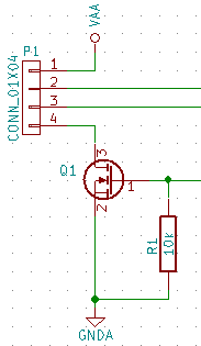
Low-Power
The ability to turn off the strain gauge network was implemented using an N-channel MOSFET on the low-side
which is driven directly by a microcontroller pin. The microcontroller pin also has an RC circuit directly
on its output in order to ensure that the analog side of the board is not 'contaminated' with conducted switching
from the digital side. This pin is not intended to be switched at high frequency, but I thought it best to
be cautious when dealing with 24 bits of resolutions since I don't have any experience beyond 12 bits.
<
SPI
I thought that it would be nice if the interface supported SPI as well as the UART. The UART is great for general purpose connections, but can be problematic if there are multiple sensors involved, which SPI can solve quite nicely. In addition, the SPI interface can support much faster transfer rates, if required.
There may be a need to 'slow down' the SPI interface using a 'data ready' output or similar. The analog SIGN output
may be multiplexed for this purpose, if necessary, to give sufficient time for the SPI request to be received, processed,
and the appropriate data placed on the SPI bus for consumption.
Analog
The simplest options is - of course - a direct analog output. In truth, this wasn't a design goal at the outset, but there were a couple of pins left, one of which could output PWM signals. I decided that a couple of RC pins would be easy to put on the board to give an analog output option. Of course, this would be the lowest resolution output, but might be pretty nice when viewing data using an oscilloscope.
The analog output is 'zero-referenced', meaning that any deviation from zero will be output as a positive number. I have done this because I hate dealing with analog outputs and the errors caused by reading the A/D with 1.65V corresponding to zero. To compensate, I have dedicated a pin to the analog 'sign' as well. This pin will be '0' when the analog voltage is negative and '1' when it is positive.
Low Noise
In order to reduce the noise of the input, we have separated out the analog and digital supplies using an RC filter on the power supply input leads:

This simple circuit has a cutoff frequency of ~79Hz. This may end up being modified to something less than 50Hz/60Hz so typical in many operating environments, but only testing can tell. The best-case scenario would probably be to add a couple of inductors in place of the resistors, but to get significant performance from an inductor requires a much larger package than a resistor, so I would like to give this a try as a 'first time out' approach. If it isn't enough, then I will modify the R value or the component.
The SparkFun board uses an HX711 chip, which claims at the header "Simultaneous 50 and 60Hz supply rejection". I'm sure that anyone reading this has seen the effects of 50Hz and 60Hz environmental noise, but I wasn't quite sure how to do this without implementing two notch filters, one at 50Hz and one at 60Hz, which could turn out to be physically large at those low frequencies. As I am trying to minimize component count, I decided to see how it goes without the filters for the first go-around. If it doesn't work out, then I will first try to do it in software. If that doesn't work, then I may try to get it done with a special-footprint PSU.
Crystal
This microcontroller can operate at 12MIPS, so I opted to go for a small 12MHz crystal. Most of this series can operate at 16MIPS, so this was somewhat of a surprise. I wanted to get the maximum speed possible since I am going to be attempting to implement an SPI slave, which requires speed.
Layout
I actually spent a lot of time on figuring out the form factor for the layout. My first layout separated out each interface on its own header, which is clean, but isn't compatible with any sort of standard. The layout was also quite small and breadboard-compatible, but didn't have some other features that I liked.
I settled on the form factor used by the Moteino. There are a couple of reasons that I did this:
- breadboard compatible
- small form factor
- anticipate a wireless application in the future
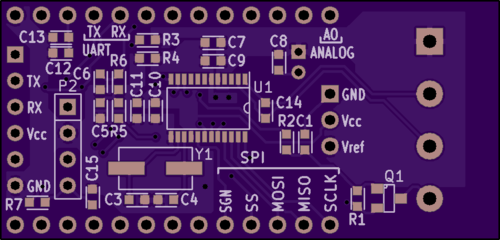

You can see that I added screw terminals to the left side (bottom pic) of the board for attachment. All SMT components are on the 'top' while through-hole components are on the 'bottom'.
In truth, laying out the board in this fashion was actually quite challenging. I had some trouble keeping the analog and digital domains far from one another and I am hoping that I didn't hobble the performance of the ADC. You can see - for instance - that the SPI outputs are pretty close to the analog side. If I see that there is noise on the ADC for this reason, then I will probably re-layout with separate interfaces and a much cleaner (electrically) layout.
For the moment, I haven't implemented any type of mounting features, but that may change in the future as well.
Software
There is currently no software written for the platform, but I am foreseeing something like a standard serial interface for configuration and crude visualization, much like the OpenScale interface. I imagine that most applications will use a low-speed UART to configure the board and use the SPI interface for high-speed access. I am considering making the sign bit configurable as the sign bit for the analog output OR as a 'data ready' output for the SPI port. This seems like a good idea since it can keep the host interrupt-driven.
Initially, I don't believe that I would like to implement an EEPROM-like ability to persist configurations through a reset, but that may change. I anticipate that most applications involving this board - at least, anything I'm working with - will be software based and - thus - easily configured on power-up. Of course, this could easily change.
I expect the software to be something like:
- initialize peripherals/hardware with defaults
- wait for A/D time
- turn on strain gauge, wait to stabilize, measure
- turn off strain gauge
- go back to '2'
In parallel, the UART would be interrupt driven, being used for configuration and/or low-speed data transmission.
Summing Up
This should be a fun project that will have a lot of applications to play with. If we can get the interface right, it should be quite easily integrated into other projects that I have in mind.
As always, check out our github repository.
- article
- current-sensor
- curve-tracer
- dispatch
- fan-controller
- fixed-point-math
- load-cell-sensor
- meta
- reference


 RSS
RSS
2
assembly
5
buffer
31
c
3
current sensor
28
curve tracer
2
fan controller
6
fixed-point math
4
interrupt
3
KiCAD
3
labview
5
layout
6
msp430
4
pelican
18
pic24
29
project
12
python
2
Q1.15
4
schematic
10
serial
3
solidworks
2
task manager
2
theme
3
tkinter
9
uart
9
xc16