-
 Project Curve Tracer - ADC Input
- Date Wed 02 March 2016
- By Jason Jones
- Category curve-tracer
- Tags curve-tracer adc c curve tracer pic24 project xc16
Intro
Up to this point, we have focused on generating signals without necessarily observing those signals. In this post, we will begin to give the microcontroller the capacity to observe those signals using the Analog-to-Digital Converter (ADC).
ADC Requirements
There are 5 signals to be observed:
- LD_VOLTAGE_0 - this is the 'high-side' voltage of the load
- LD_VOLTAGE_1 - this is the 'low-side' voltage of the load
- CURRENT - this is the output of the U1 circuit, which is a voltage proportional to the load current
- HZ_OUT_1 - this is the bias voltage of the differential opamp
- HC_OUT_2 - this is currently unused, but will eventually be the bias voltage for the base/gate drive circuit
Ideally, all of these signals would be simultaneously sampled. Unfortunately, we don't have that capability, but we do have a reasonably fast A/D converter at 100k samples/s. If we run the A/D at maximum speed, we can achieve 10μs spacing between each sample and have a complete dataset every 50μs, which limits our maximum possible sample rate to 20kHz. The highest sample rate that we require is at the Timer 1 frequency used to generate the DAC signal. In the DAC post, we found that the frequency of T1 which generates a pretty good waveform is 1.3kHz, so this is well within the capabilities of a 20kHz ADC.
Setting Up
Following the Example
I like to start at a 'known good' place. I went to the Microchip site for this processor, down to documentation, and looked at the A/D document. They had Example 51-6, which is supposed to set up the converter to sample/convert a single channel continually:
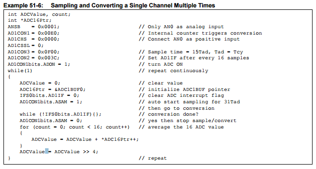
Unfortunately, the example doesn't work. In AD1CON1, they have a value of 0x00E0 whereas a value of 0x0070 is what you require in order to use the internal counter to trigger the conversion.
I started using the sample code for setup, but instead of placing all of the garbage that they have in the 'while' loop, I placed the portion that I require into an interrupt. I also set up the initialization to start on channel 1 instead of channel 0. I wrapped all of this up and placed it into a function 'initAdc()'.
1 2 3 4 5 6 7 8 9 10 11 12 13 14 15 16 17 18 19 20 21 22 23 24 25 26 27 28 29 30 | void initAdc(void){
/* set up the analog pins as analog inputs */
TRISAbits.TRISA1 =
TRISBbits.TRISB0 =
TRISBbits.TRISB4 =
TRISAbits.TRISA4 =
TRISBbits.TRISB6 = DIO_INPUT;
ANSAbits.ANSA1 =
ANSBbits.ANSB0 =
ANSBbits.ANSB4 =
ANSAbits.ANSA4 =
ANSBbits.ANSB6 = DIO_ANALOG;
AD1CON1 = 0x0270; /* Internal counter triggers conversion
* FORM = left justified */
AD1CON2 = 0x003C; /* Set AD1IF after every 1 samples */
AD1CON3 = 0x0107; /* Sample time = 1Tad, Tad = 8 * Tcy */
AD1CHS = CURRENT_VOLTAGE_AN; /* AN1 */
AD1CSSL = 0;
AD1CON1bits.ADON = 1; // turn ADC ON
AD1CON1bits.ASAM = 1; // auto-sample
/* analog-to-digital interrupts */
IFS0bits.AD1IF = 0;
IEC0bits.AD1IE = 1;
return;
}
|
As I mentioned, I also enabled interrupts in order to refrain from polling the interrupt flag. I looked up the function for ADC interrupts in the Microchip docs and cleared the interrupt flag within it:
1 2 3 4 5 | void _ISR _ADC1Interrupt(void){
/* clear the flag */
IF0bits.AD1IF = 0;
}
|
We will do more than this in the future, but it is a good start. Once we get here, we can set a breakpoint at the only line within the function and run the processor using the debugger. If all is well, we should hit the breakpoint every time we press 'play'.
Calculating Values
At this point, we should diverge a bit to talk about the calculated values that we wish to see from the A/D. Our A/D is configured to be a left-aligned unsigned value. To become a signed value, we can simply shift the value by one to the right in order to leave room for a sign bit. This will be useful for calculations later on.
First off, we want to know the differential voltage across the load and across time. This involves measuring the low-side voltage of the load and subtracting it from the high-side voltage of the load and then saving that value into an array.
- loadVoltageL = AdcLoadL >> 1
- loadVoltage[sampleIndex] = (AdcLoadH >> 1) - loadVoltageL
The next value that we want to save is the current value across time. The value of the current is measured instantaneously and requires subtraction of the HZ1 voltage as the reference of the opamp circuit. The time will be saved as an array that is indexed in the same way that the load voltage is indexed.
- loadCurrent[sampleIndex++] = (AdcLoadCurrent >> 1) - hz1Value
Finally, the two HZ outputs must be measured and saved.
Moving Through the Inputs
Unfortunately, there is no mode that will automatically load the A/D values into their proper places and then trigger the interrupt in this processor. There are other chips in this line that will, but we don't have one. As a result, we will have to manually multiplex the A/D to the proper channels.
Since we can't simultaneously sample the channels, we would like to sample the high-side voltage, low-side voltage, and current as closely together as possible. We will then sample the HZ outputs.
We must change the 'trigger' source to when the SAMP bit is cleared instead of on a timer in order to remain synchronous. At the end of the T1 interrupt, we will clear the SAMP bit. On each source, we will change the source and, again, clear the SAMP bit. At the end of the chain, we will not clear the SAMP bit again until the next T1 interrupt. Only three lines change significantly in the initAdc() function:
1 2 3 | AD1CON1 = 0x0200;
AD1CON2 = 0x0000;
AD1CON3 = 0x0007;
|
The _T1Interrupt() function gets one line added to the end of it to clear the SAMP bit:
1 2 3 4 5 6 7 8 9 10 11 12 | void _ISR _T1Interrupt(void){
static q16angle_t theta = 0;
theta += omega;
DAC1DAT = q15_fast_sin(theta) + 32768;
DAC2DAT = q15_fast_sin(theta + 32768) + 32768; // theta + 180 deg
IFS0bits.T1IF = 0;
AD1CON1bits.SAMP = 0; // <= Added this line
return;
}
|
Finally, a switch/case statement gets added inside the A/D interrupt in order to change the input channel being sampled and to properly clear the SAMP bit:
1 2 3 4 5 6 7 8 9 10 11 12 13 14 15 16 17 18 19 20 21 22 | void _ISR _ADC1Interrupt(void){
switch(AD1CHS){
case LD_VOLTAGE_1_AN:
{
loadVoltageL = (q15_t)(ADC1BUF0 >> 1);
AD1CHS = LD_VOLTAGE_0_AN;
AD1CON1bits.SAMP = 0;
break;
}
case LD_VOLTAGE_0_AN:
{
loadVoltage[sampleIndex] = (q15_t)(ADC1BUF0 >> 1) - loadVoltageL;
AD1CHS = CURRENT_VOLTAGE_AN;
AD1CON1bits.SAMP = 0;
break;
}
case CURRENT_VOLTAGE_AN:
/* ... more code follows... */
|
Of course, more case statements follow, but they all look nearly identical except for the last one, which does not clear the SAMP bit.
Adjusting T1 Frequency
I would like for all ADCs to be sampled after the T1 interrupt. As a result, The period of the T1 interrupt must be longer than the time to sample and convert 5 A/D cycles. As each A/D cycle takes \~10μs and our current T1 period of '250' corresponds to 15.625μs, we will have to increase our T1 period to '1000' in order to pack all A/D sample and conversion cycles into the span of a single T1 interrupt.
Results
After going through all of this setup and playing, it is time to test. I have set the LATB7 bit at the beginning of the A/D interrupt and cleared it at the end of the interrupt in order to get a visualization of when the A/D interrupt is executing relative to the T1 interrupt.

In the scope capture, you can see in blue the output waveform. Each transition of that waveform to a different level marks the T1 interrupt and, thus, the clearing of the SAMP bit. Each yellow positive transition marks the 5 A/D interrupts that are triggered by the T1 interrupt.
After running the code and plotting the load voltage and the current arrays:
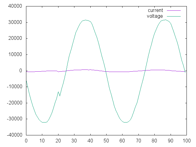
The discontinuity is where the index was loading values, so the most recent value loaded was actually sample 20. We will make efforts to fix this in later segments.
Summary
Now we have most of the blocks of the core waveform generator and A/D functioning as expected. We will probably tighten up a couple of blocks in preparation for UART transmission of data in the next segment.
As always, you can find our the code in our github repository.
- article
- current-sensor
- curve-tracer
- dispatch
- fan-controller
- fixed-point-math
- load-cell-sensor
- meta
- reference


 RSS
RSS
2
assembly
5
buffer
31
c
3
current sensor
28
curve tracer
2
fan controller
6
fixed-point math
4
interrupt
3
KiCAD
3
labview
5
layout
6
msp430
4
pelican
18
pic24
29
project
12
python
2
Q1.15
4
schematic
10
serial
3
solidworks
2
task manager
2
theme
3
tkinter
9
uart
9
xc16