-
 Project Curve Tracer - Schematic Errors
- Date Thu 25 February 2016
- By Jason Jones
- Category curve-tracer
- Tags curve-tracer curve tracer layout pic24 project schematic
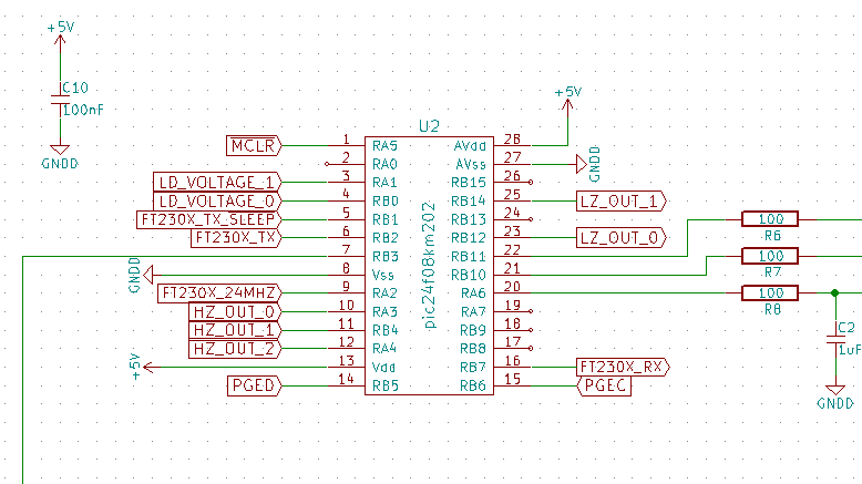
As always, there are some schematic errors. This is one of the issues with highly integrated ICs, it is so easy to mix up the pins! Maybe I should stop doing schematic and layout so late at night...
- Vcap should be on pin 20, nothing else. This error arose from me reading the wrong columns in the data sheet. We simply have to solder a 4.7uF cap across R8 and short C2. We also have to cut the trace going to the U1 circuit and attach that trace to the identical circuit on R7.
- LZ_OUT_x pins were intended to be the operational amplifier outputs. Instead, they are the DAC outputs. The opamp outputs are on pins 7 and 26. Pin 7 currently holds the current sense A/D input and will have to have the trace cut and a patch wire added to another A/D. Pins 25 and 26 can probably be easily jumpered with a solder bridge if pin 25 is made to be an input.
- The programming header has pins 1 and 2 swapped.
This is much more rework than is typical for my layouts, but with boards costing less than the parts on it, it isn't a big deal. We will continue to patch the boards we have - and post embarassing pictures - until we have a fully functioning layout! I'm sure that more problems are waiting to be found.
- article
- current-sensor
- curve-tracer
- dispatch
- fan-controller
- fixed-point-math
- load-cell-sensor
- meta
- reference


 RSS
RSS
2
assembly
5
buffer
31
c
3
current sensor
28
curve tracer
2
fan controller
6
fixed-point math
4
interrupt
3
KiCAD
3
labview
5
layout
6
msp430
4
pelican
18
pic24
29
project
12
python
2
Q1.15
4
schematic
10
serial
3
solidworks
2
task manager
2
theme
3
tkinter
9
uart
9
xc16